- Automobiles & Motorcycles
- Beauty & Personal Care
- Business Services
- Chemicals
- Construction & Real Estate
- Consumer Electronics
- Electrical Equipment & Supplies
- Electronic Components & Supplies
- Energy
- Environment
- Excess Inventory
- Fashion Accessories
- Food & Beverage
- Furniture
- Gifts & Crafts
- Hardware
- Health & Medical
- Home & Garden
- Home Appliances
- Lights & Lighting
- Luggage, Bags & Cases
- Machinery
- Measurement & Analysis Instruments
- Mechanical Parts & Fabrication Services
- Minerals & Metallurgy
- Office & School Supplies
- Packaging & Printing
- Rubber & Plastics
- Security & Protection
- Service Equipment
- Shoes & Accessories
- Sports & Entertainment
- Telecommunications
- Textiles & Leather Products
- Timepieces, Jewelry, Eyewear
- Tools
- Toys & Hobbies
- Transportation
Summarize 10 PCB component placement tips
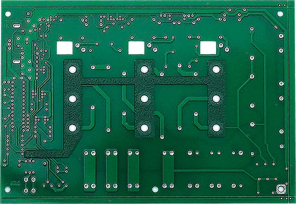
Printed circuit boards (PCBs) are by far the most common method of assembling modern electronic circuits. Composed of a sandwich of insulating layer (or layers) and one or more copper conductor patterns, they can introduce various forms of errors into a circuit, particularly if the circuit is operating at either high precision or high speed. PCBs, then, act as “unseen” components wherever they are used in precision circuit designs.
1. Why is effective component wiring layout important?
You're happy when you're placing components on a PCB based on your whims and fantasies, but you're unhappy when something goes wrong in the field and you're faced with a barrage of complaints and flak from other engineers and customers.
Improper placement of components can affect features such as functionality, durability, manufacturability, and maintainability of the PCB. For example, place analog and digital components without proper isolation, and congratulations, you have perfectly and successfully compromised analog signals.
Lack of functionality isn't the only problem when components are placed incorrectly. If you are designing a PCB that requires regular maintenance, if there is a problem with component placement, congratulations again, you will be "loved" by on-site maintenance personnel.
2. Common PCB component placement issues
Generally speaking, most component placement issues occur due to more complex wiring or other issues. Here are some common problems:
The distance between components is too close
When components are placed too close together, automatic pick-and-place issues can occur, adversely affecting the test (fixture).
It is inconvenient to separate PCB panels
When components are too close to the edge of the board, it can be difficult to use routing to separate the PCB panel into single boards.
Rework becomes more difficult
If rework is required, it will be more difficult if the components are not well spaced.
Position and direction of wave soldering components
If the components are discrete, when the PCB goes through wave soldering, both pins go into the solder at the same time. However, for larger components, they should not be placed in front of larger components because shadows will be produced.
3. PCB component placement skills
Understand the shape and size restrictions of PCB boards
When designing a PCB, the most important thing to consider is the enclosure within which the PCB will need to be mounted, determining the location of mounting holes and edge connectors, which are critical to the shape and size of the PCB.
Understand the manufacturing process of PCB board
Before designing a PCB board, you need to consult the PCB manufacturer on what processes are used to assemble and test the PCB and components, and determine the space you will occupy on the PCB board.
Do not place integrated circuits too close to each other
It is recommended to leave at least 0.35 inches to 0.5 inches of spacing between each integrated circuit on the PCB board, with more space for larger ICs. Placing ICs too close results in limited space when routing connecting pins, which wastes time rearranging the design.
4. Make sure similar components face the same direction
Orienting similar components in the same direction makes installation, inspection, and testing easier for subsequent personnel. Failure to orient similar components in the same direction can disrupt the soldering process or even result in some components not being soldered at all, which can lead to shorts and opens on the PCB.
Further reading:Why Choose Carbon Film Resistors?
NTE Electronics 1/4 Watt 4.7K OHM Resistor 4-Pack
5. Group components by function
Make sure components are segregated according to functional blocks in the circuit. For example, power management components should not be mixed with analog components, and high-speed digital communications should remain separate.
Plan where these components should be placed on the PCB. A rule of thumb is to keep the noisiest signals away from highly sensitive signals. Additionally, by grouping components according to function, you can better control their return paths.
6. Place edge components first
Placing edge components facilitates board layout for input and output connections. These are usually parts that cannot be moved due to the mechanical housing (e.g., connectors, switches, jacks, USB ports, etc.). If you do this, trust me, PCB installers and technicians will be grateful.
7. Positioning of high-frequency components
When electrical signals exceed frequencies of 1 MHz, the system becomes very critical, especially in the positioning of electrical and electronic components, especially capacitive and inductive components. Even when electrically connected to each other, these components can behave differently depending on their arrangement, shape and size of the electrical connections. Sometimes moving a capacitor or inductor just a few centimeters is enough to completely change the behavior of an electronic circuit.
In high-frequency circuits, the ground plane must be very limited in its extension and the components connected to it should be as close to each other as possible.
8. Place cooling components
A general rule states that the traces connecting various components (resistors, capacitors, inductors, integrated devices, etc.) should be very short and the devices very close together. This is indeed the case when operating primarily at high frequencies. However, minimizing the length of a connection can create thermal issues, leading to uneven accumulation of localized heat.
Faults that at first glance cannot be explained, in these cases it is better to adopt the parallel positioning of the components and heat pipes in the circuit.
9. Keep components away from heat dissipation areas
In applications with high power requirements, the voltage regulator can heat up significantly. Most likely, you've included some thermal vias to increase heat dissipation. However, placing other components near the regulator is less tactful. The same applies when you're using a power op amp or other heat-generating device.
10. Place all components on the same layer as much as possible
Many designs require multiple layers PCBs on one layer to accommodate weight and space constraints. However, if the parts are placed on multiple layers, double multi-channel must not be performed due to soldering process issues when mounting components, which may waste unnecessary expensive manufacturing costs.
Placing components in logical groups on the PCB layout like a schematic design will save time and minimize trace lengths because many parts are already logically grouped based on the schematic.
The above is a brief introduction to PCB component placement techniques, I hope it will be useful to everyone.
If you are interested in sending in a Guest Blogger Submission,welcome to write for us!


Comments
0